
Add : 1303 Room Fengsheng Building 51# Xinsha Road S.Z
Tel : +86-755-3698 9407
Fax : +86-755-3698 9408
Mobile : +86-185 0307 7246
E-mail : tommy@PcbFpcBoard.com
Website : www.pcbfpcboard.com
NEWS
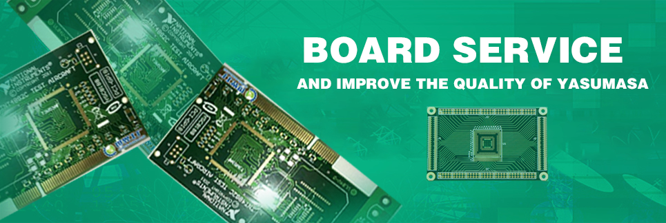
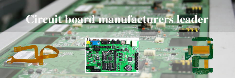
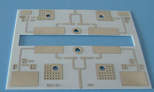
Driven by miniaturisation of electronics products, microvia and fine-line technologies are the key technologies for 21st High Density Interconnect (HDI) manufacture in PCB and Electronics industries. Microvia ablation has been attractive for its speed and throughput. However, the drawback has been the additional photoimaging process to etch the via pattern. Work is needed to develop and apply HDI ablation technique without etching via pattern (conformal mask). A set of practical processing windows are necessary, which will be developed and customized in different manufacturing sites. HDI imaging enables fine-line pattern (under 50um) to be formed on PCB and electronics substrate. It also shows reduction in process steps versus conventional contact imaging. However, to promote and transfer this technology, productivity and quality are important factors. Study on comparison of quality between conventional contact imaging and HDI imaging will be needed. Factors affecting throughput will be studied. Investigation on the effect of energy requirement on feature size has also to be carried out. This project helps local PCB and electronics substrate industries to establish and elevate its necessary technical competency for survival and to enhance its productivity and quality. This elevation in technology eventually increases competitive edge and also promote awareness on innovation development within these industries. In the near future, these industries shall be able to develop their own technology niches and excel in some of the major technological areas.
Previous : Development Plasma treatment for PCB fabrication process
Next : Development of the PCBs
